
Latest News
-

-

Rockchip RK3568 External SD Card Design
2025-02-13 -

-

Rockchip RK3568 mSATA Hard Drive Solution
2025-02-12 -

Rockchip RK3568 USB3.0 HOSTA Schematic and Layout Design Guide
1. Overview
The Rockchip RK3568 is a high-performance, low-power processor widely used in smart terminals, edge computing, and other fields. Its built-in USB3.0 controller supports the USB3.0 HOSTA interface, providing data transfer rates of up to 5Gbps. This article details the schematic design and layout considerations for the RK3568 USB3.0 HOSTA interface based on the WTC-RK3568S core board from Weathink, helping developers achieve stable and reliable USB3.0 connections.
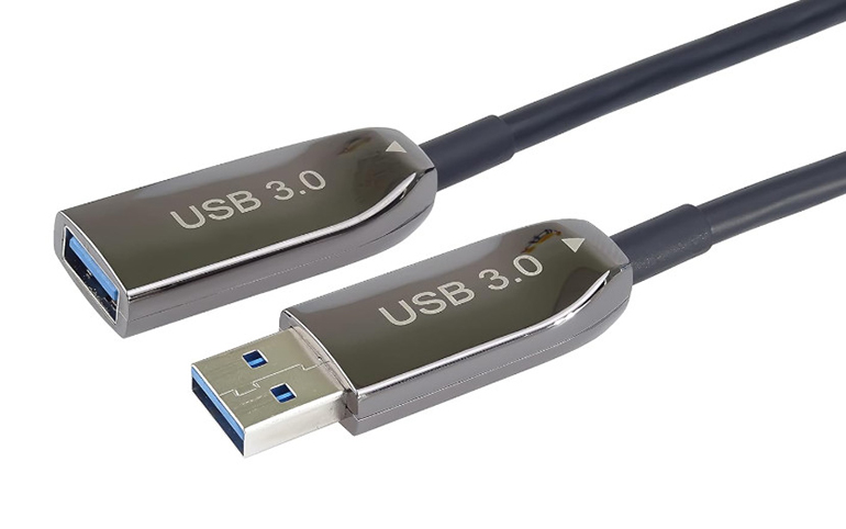
Figure 1: USB3.0 HOSTA
2. Schematic Design
2.1 Power Design
VBUS Power Supply: The USB3.0 HOSTA interface needs to provide VBUS power to connected devices, typically at 5V. It is recommended to use an independent DC-DC power chip for VBUS supply, with sufficient current margin (at least 1A).
2.2 Signal Connections
Differential Signal Pairs: The USB3.0 HOSTA interface includes two differential signal pairs: TX+/TX- and RX+/RX-. Ensure that the differential signal pins of the RK3568 USB3.0 HOSTA interface are correctly connected to the corresponding pins of the USB connector.
Single-Ended Signals: The USB3.0 HOSTA interface also includes single-ended signals such as VBUS, D+, D-, ID, and GND. These signals must be correctly connected to the corresponding pins of the USB connector.
2.3 ESD Protection
To enhance the ESD protection capability of the USB3.0 HOSTA interface, it is recommended to add ESD protection devices, such as TVS diodes, on the differential signal lines. Additionally, adding 2.2Ω resistors on the D+ and D- signal lines can provide some protection for the chip. All signals on the USB3.0 connector must include TVS diodes, which should be placed as close as possible to the USB connector. For SSTXP/N and SSRXP/N signals, the maximum junction capacitance of the TVS diode should not exceed 0.4pF.
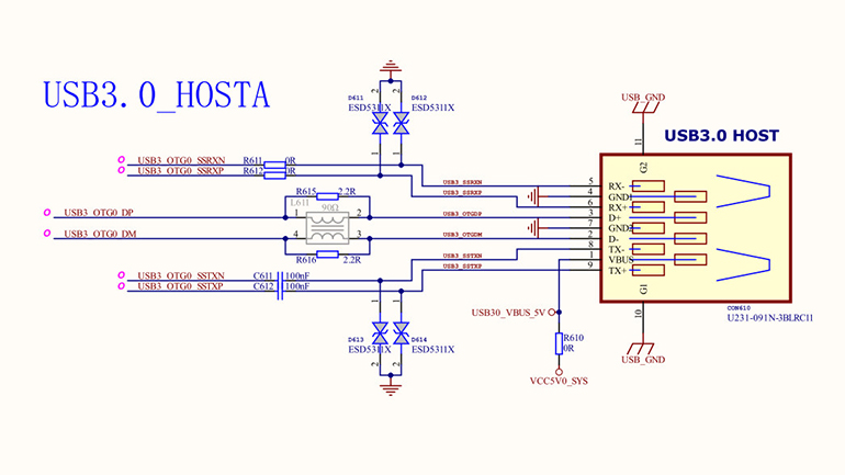
Figure 2: RK3568 USB3.0 Connection Diagram
3. Layout Design
3.1 Differential Signal Routing
●Impedance Control: The characteristic impedance of USB3.0 differential signals is 90Ω. Use impedance calculation tools to determine the width and spacing of PCB traces and verify with impedance testing instruments.
●Length Matching: SSTXP/N and SSRXP/N differential pairs must strictly follow differential routing rules. For example, they must maintain the same length, width, layer, and fixed spacing, and should be as symmetrical as possible. The intra-pair length mismatch should be controlled within 12 mils.
●Minimize Vias: Reduce the number of vias on differential signal lines as much as possible, as vias introduce impedance discontinuities and signal reflections. SSTXP/N and SSRXP/N should ideally be routed on the top layer. If layer changes are necessary, use no more than two vias, and place symmetrical ground stitching vias near the signal vias. The center-to-center distance between ground stitching vias and signal vias should not exceed 30 mils. Use curved or obtuse angles for trace bends, avoiding right or acute angles.
Avoid Crossings: Avoid crossing differential signal lines with other signal lines, especially high-speed signals.
3.2 Power Routing
●Widen Traces: VBUS and VDDIO power traces should be widened to reduce impedance and voltage drop.
●Add Filter Capacitors: Place appropriate filter capacitors near the VBUS and VDDIO power pins to filter out power noise.
3.3 Ground Plane
●Solid Ground Plane: Maintain a solid ground plane to provide a good return path for signals. The reference layer for SSTXP/N and SSRXP/N signals must be a solid ground plane, avoiding continuous vias that could block the signal return path.
●Split Ground Plane: If splitting the ground plane is necessary, use ferrite beads or 0Ω resistors to connect different ground planes.
4. Other Considerations
●Simulation Verification: Use signal integrity simulation tools to verify the signal integrity of the USB3.0 HOSTA interface, ensuring that signal quality meets requirements.
●Testing Verification: After PCB fabrication, use instruments such as oscilloscopes to test and verify the signals of the USB3.0 HOSTA interface, ensuring compliance with specifications.
●Common Mode Choke: Reserve space for common mode chokes on USB differential signals as a means to improve EMI performance.
5. Conclusion
The schematic and layout design of the RK3568 USB3.0 HOSTA interface must follow certain specifications to ensure signal integrity and system stability. This article has introduced the schematic design, layout considerations, and other precautions for the RK3568 USB3.0 HOSTA interface, aiming to assist developers in completing related design tasks more effectively.
Hangzhou Weathink Electronics Co., Ltd., as a professional motherboard design company, has extensive experience in USB3.0 applications. Feel free to contact Weathink for our independently designed RK3568 SOM and stable, reliable industrial computers.
https://www.weathink.com/products/hexinban/13.html